| Quantity | 3+ units | 10+ units | 30+ units | 50+ units | More |
|---|---|---|---|---|---|
| Price /Unit | $351.45 | $344.28 | $333.52 | $319.17 | Contact US |
 BU-5 Bluetooth Module Radio Bluetooth Adapter Unit for Yaesu FTM-150R FTM-510DR Transceiver
$55.79
BU-5 Bluetooth Module Radio Bluetooth Adapter Unit for Yaesu FTM-150R FTM-510DR Transceiver
$55.79
 PLJ-0802-E Mini Portable 1MHz-1200MHz Frequency Measurement Module Embedded Intelligent Frequency Meter
$16.84
PLJ-0802-E Mini Portable 1MHz-1200MHz Frequency Measurement Module Embedded Intelligent Frequency Meter
$16.84
 H7 R2 0.3MP HD Smart Camera Module MT9M114 Opensource Visual Module + LCD Expansion Module Compatible with OpenMV4 H7 R2
$42.69
H7 R2 0.3MP HD Smart Camera Module MT9M114 Opensource Visual Module + LCD Expansion Module Compatible with OpenMV4 H7 R2
$42.69
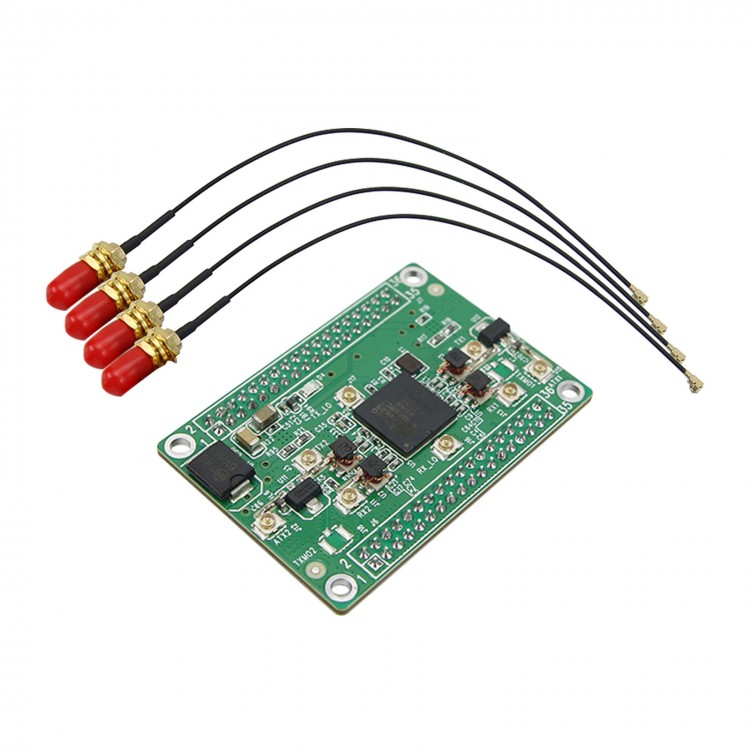
AD9361 Development Board RF Transceiver Module Software Radio SDR Wireless Data Acquisition Module
Description:
The AD9361 chip is a high-performance, highly integrated bidirectional transceiver from baseband to radio frequency (RF). The programmability and broadband capability of the device make it an ideal choice for a variety of transceiver applications. The device integrates the RF front end and the flexible mixed-signal baseband part, and integrates a frequency synthesizer to provide a configurable digital interface for the processor, thereby simplifying design import. The AD9361 operating frequency range is 70 MHz to 6.0 GHz, dual input and dual output, and the supported channel bandwidth range is less than 200 kHz to 56 MHz.
The SRF_AD9361_V2.0 software RF module is only 35mm * 50mm in size, and uses a single 5V power supply.
The principle diagram of the module is as follows:
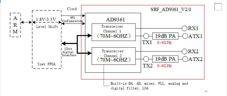
SRF_AD9361_V2.0 module principle diagram and its typical external relationship:
On the digital side, the input and output of SRF_AD9361_V2.0 are directly connected to the user's digital circuit, generally FPGA and ARM, and the logic level is 1.8V. In addition to the clock, it includes an SPI interface and a 12-bit user baseband interface. On the radio frequency side, the input and output interfaces of SRF_AD9361_V2.0 include two radio frequency input interfaces RX1 and RX2, two radio frequency output interfaces TX1 and TX2 directly connected to AD9361 (the signal range of TX1 and TX2 is 0MHZ-6GHZ), TX1 and TX2 The typical maximum output is 0dBm, which is used to connect with the power amplifier that the user may have.
In order to reduce the workload of users, we also integrated a 19dBm power amplifier on SRF_AD9361_V2.0, which is convenient for most users to use directly under laboratory conditions. ATX1 and ATX2 are the output after power amplification. The working range of the power amplifier is 0-4GHz.
The external interface of the module is as follows:
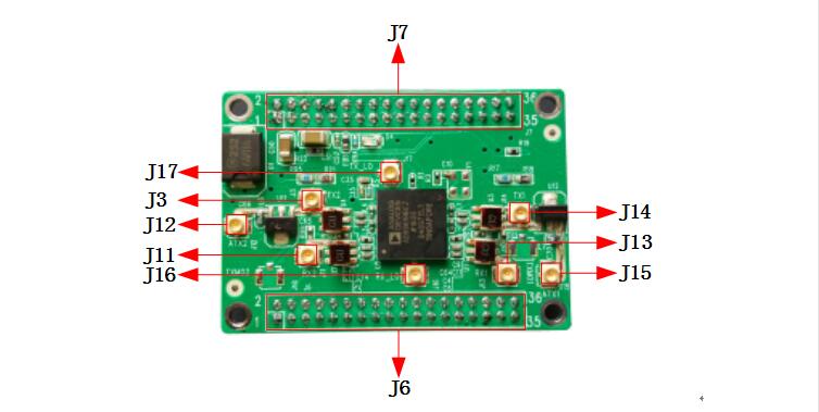
Among them, J6 and J7 are the power supply and digital circuit interface of the module, which is composed of two 18 * 2 pin headers with a pin spacing of 2mm, leading to all the digital interfaces of the AD9361. The power supply is 5V DC.
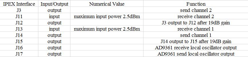
The input and output of the module's RF signal are connected to the outside through the IPEX interface. The following table shows the description of each IPEX interface.
Package Included:
1 x AD9361 Development Board