| Quantity | 3+ units | 10+ units | 30+ units | 50+ units | More |
|---|---|---|---|---|---|
| Price /Unit | $146.26 | $143.27 | $138.79 | $132.82 | Contact US |
 TPA3255 High Performance Class D Power Amplifier Board 2.0 Channel Mini Digital Audio Stereo Amplifier Module
$26.56
 HiFi UCD700 Fully Discrete Power Amplifier Board 700W Digital Mono Class D Audio Amplifier Module
$34.90
 UCD400 Multifunctional Power Amplifier Board Class D HiFi Audio Amplifier Module for HYPEX
$95.38
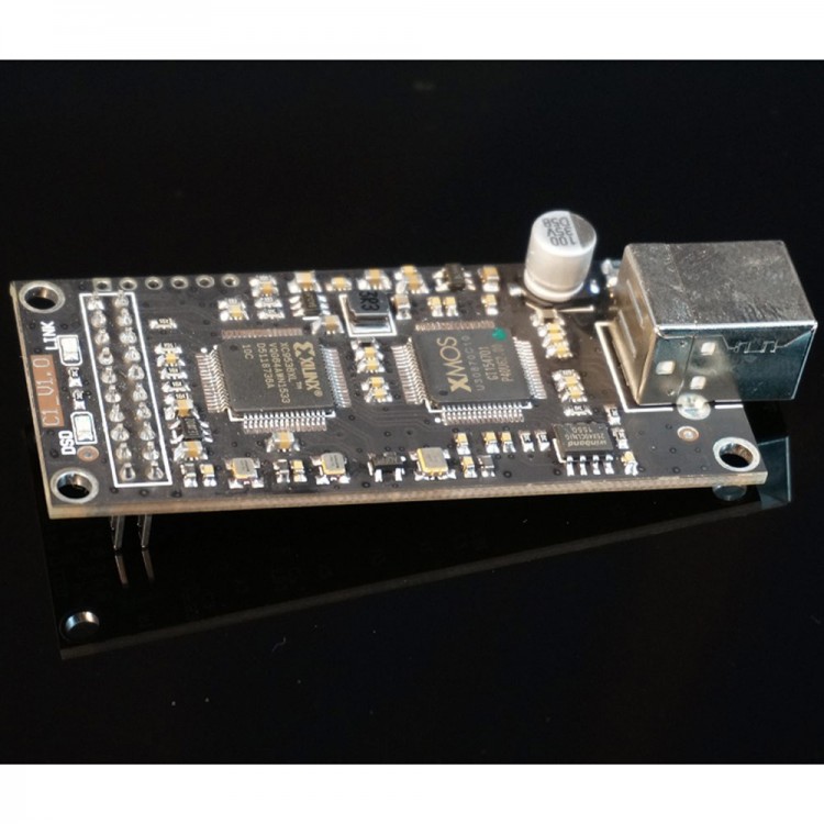
C-1 XMOS Digital Interface XU208 U8 Upgraded Version Femtosecond TCXO for Audio Amplifier
Drive and more information: Click here
Description:
C-1 is our team developed a high-performance digital interface USB digital audio interface,adopted the latest XMOS xCORE - 200 series chips.C-1 is a low jitter clock system of digital interface.C-1 digital interface with a standard usb input interface,and F-1 has a lot of output interface,including I2S interface.
Technical Features:
- C-1 is a the XMOS latest xCORE - 200 series of high-end products USB digital interface.A new generation of XMOS chip,using the more advanced process technology,the performance than the old one U8 chip doubled,the processing capacity of up to 1000 MIPS.
- It is well known that the weight of the core of the digital audio is algorithm.Our team work in the field of digital audio for many years,at the same time get XMOS detailed FAE team's strong support,we are on the basis of the original firmware had done many of the technical improvement and optimization algorithm.
Technical indicators:
Each output interface to support the sampling rate of:
- PCM:44.1KHz,48KHz,88.2KHz,96KHz,
- 176.4KHz,192KHz,352.8KHz,384KHz
- DSD: 2.8 MHz (DSD64) - DoP,native
- 5.6 MHz (DSD128) - DoP,native
- 11.2 MHz (DSD256) - DOP,native
- A wide:top 32 bit over I2S output
- The highest bit over 24 S/PDIF
- Screw I2S row needle position is fully compatible with Italian Amanero module;The whole plate adopts the design of the three crystals,including audio crystals for customised version FeiMiaoJi crystals,SMT packaging small volume.
Each interface electrical standards:
- USB input socket for standard USB - type B mother,USB power supply range is 4.5 V to 4.5 V;
- RCA S/PDIF signal output interface standard,level of 550 mv(standard load),the output impedance of 75 ohms.
Design details:
1. Electricity is the mother of the sound implementation of the design concept,attaches great importance to the power circuit design,USES the high performance,low noise and has fast response "as the main power supply.Whole board USES two-way independent power supply, "the clock part they even adopted the ADI ultra low noise, in order to ensure the output performance has laid a solid foundation to the extreme
2. PCB board USES 4 layer PCB design,make sure you have complete ground plane and the power supply layer,adopting high speed digital design method, ensure the whole signal integrity and power integrity.The clock signal for special processing,using the impedance of the package design and precise control,so as to ensure the quality of the clock signal and improve its anti-interference ability.Input and output signals are all follow the standard design,especially the USB high speed signal using the 90 ohms difference impedance control.
System compatiblity:
- Windows XP, Windows 7,Windows 8,Windows 10; 32/64 bit
- Native MacOS 10.6 and later,use driver of your system
- Native Linux with UAC2 compliant kernel,use driver of your system
- Android OS 4.2 and upper,need device that supports OTG,and Android 5.0 is default,please use suitable player if below Android 5.0
I2S socket output signal instruction:
- High electrical level MUTE,DSD ON is DSD date streams when high electrical level.
- All electrical levels are LVCMOS,voltage is 3.3V.
- 3.3+ is output power supply,and output electric current is lower than 50mA.
- MCLK output is 22.5792Mhz or 24.576Mhz clock.
- FS0,FS1,FS2 is sampling rate indicate elctricity level,FS3 not.
Package List:
- 1 x Module