| Quantity | 3+ units | 10+ units | 30+ units | 50+ units | More |
|---|---|---|---|---|---|
| Price /Unit | $114.40 | $112.06 | $108.56 | $103.89 | Contact US |
 BU-5 Bluetooth Module Radio Bluetooth Adapter Unit for Yaesu FTM-150R FTM-510DR Transceiver
$55.79
 STF10M1000M-25 RF Power Amplifier 10-1000MHz 25W-30W Wideband RF Amplifier without Radiator and Cooling Fan
$490.69
 STF10M1000M-25 RF Power Amplifier 10-1000MHz 25W-30W Wideband RF Amplifier with Radiator and Cooling Fan
$543.48
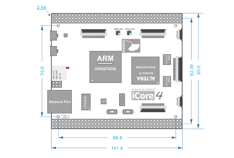
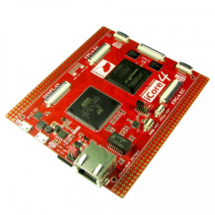
Dual-Core Industrial Control Board STM32 Development Board For ARM + FPGA (Industrial Grade)
Comparison of Quasi-Industrial and Industrial Versions:
- Quasi-industrial Grade: FPGA model is EP4CE15F23C8N. FPGA operating temperature range is 0℃ to 80℃.
-
Industrial Grade: FPGA model is EP4CE15F23I7N. The operating
temperature range of the FPGA is -40℃ to 105℃. The other chips of the
two versions are exactly the same.
Description:
Super performance, practical dual-core industrial control board.
Technical Parameters For iCore4:
1. A new combination for ARM + FPGA dual-core, strong combination;
2. For ARM, selects high-performance M7, the model is STM32F767IGT6, 176-pin, and has more resources;
3. FPGA selects EP4CE15F23C8N, 484-pin;
4. The PCB is a six-layer circuit board;
5. For ARM external expansion 32MB SDRAM, can be used as display cache;
6.
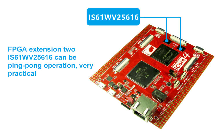
FPGA external expansion dual chip 61WV25616 (100M working frequency,
512KB size), can be used for ping-pong operation; very practical;
7. FPGA dual clock input, 24M / 25M, more convenient for application;
8. Built-in USB-TTL, it can display debug information when directly connected to a computer;
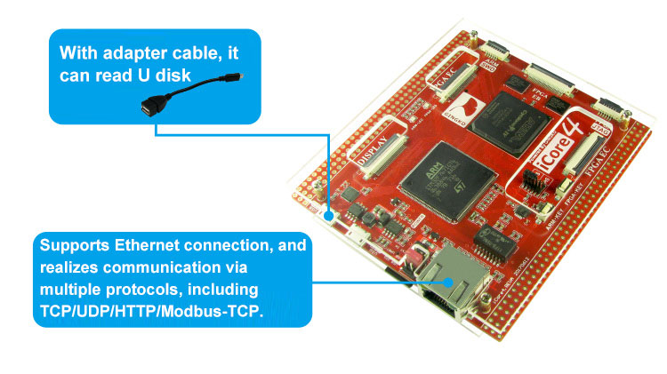
9. 100M high-speed Ethernet;
10. USB2.0 high-speed USB 2.0 OTG interface, the speed is over 40MB; you can also read U disk;
11. Support for ARM to configure FPGA, and can also support remote configuration of FPGA through Ethernet, usb, TF card, etc .;
12.
Comes with display drive interface, supports 4.3-inch, 5-inch and
7-inch display screens through the transfer; the most supported
resolution is 1024x768;
13. Up to 200+ FPGA IO interface leads;
14. Built-in practical current and voltage monitoring circuit.
For iCore4 Basic Experiment Routine:
Routine For ARM [Updating]
Routine 1: ARM driving three-color LED
Routine 2: read the ARM key state
Routine 3: EXTI interrupt experiment-read ARM key state
Routine 4: USART experiment-control LED status by command
Routine 5: SYSTICK timer experiment-light LED regularly
Routine 6: IWDG watchdog experiment-reset ARM
Routine 7: WWDG watchdog experiment-reset ARM
Routine 8: timer PWM experiment-breathing light
Routine 9: ADC experiment-power supply monitoring routine
Routine 10: RTC real-time clock experiment-display time and date
Routine 11: DMA experiment-memory to memory transfer
Routine 12: General timer experiment-LED lighting regularly
Routine 13: SDIO experiment-read SD card information
Routine 14: FATFS experiment-file operation
Routine 15: USB_CDC experiment-high-speed data transmission
Routine 16: USB_HID experiment-two-way data transfer
Routine 17: USB_MSC experiment-read / write U disk (large capacity memory)
Routine 18: USB_VCP experiment-virtual serial port routine
Routine 19: USBD_MSC experiment-virtual U disk
Routine 20: LWIP_TCP_CLIENT experiment-Ethernet data transmission
Routine 21: LWIP_TCP_SERVER experiment-Ethernet data transmission
Routine 22: LWIP_UDP experiment-Ethernet data transmission
Routine 23: LWIP_HTTP experiment-web server
Routine 24: LWIP_DHCP experiment-dynamic IP allocation
Routine 25: LWIP_DNS experiment-domain name resolution
Routine 26: LWIP_MODBUS_TCP experiment-power monitoring
Routine 27: LWIP_NETIO experiment-Ethernet speed measurement
Routine 28: FMC experiment-read and write FPGA
Routine 29: SD_IAP_FPGA experiment-update and upgrade FPGA
Routine 30: U_DISK_IAP_FPGA experiment-update and upgrade FPGA
Routine 31: HTTP_IAP_FPGA experiment-update and upgrade FPGA
Routine 32: UART_IAP_ARM experiment-update and upgrade STM32
Routine 33: SD_IAP_ARM experiment-update and upgrade STM32
Routine 34: U_DISK_IAP_ARM experiment-update STM32
Routine 35: HTTP_IAP_ARM experiment-update STM32
Routine 36: DAC experiment-output DC voltage
Routine 37: SDRAM experiment-read and write SDRAM
Routine 38: DSP MATH library test
FPGA routine [Updating]:
Routine 1: GPIO output experiment-light up LED
Routine 2: GPIO input experiment-identify button input
Routine 3: counter experiment-counter use
Routine 4: Signal TapII-logic analyzer
Routine 5: basic logic gate experiment-use of logic gate
Routine 6: Signal TapII-logic analyzer
Routine 7: basic logic gate experiment-logic gate use
Routine 8: multiplier experiment-multiplier use
Routine 9: phase-locked loop experiment-phase-locked loop use
Routine 10: FSMC bus communication experiment-multiplexed address mode
Routine 11: FSMC bus communication experiment-independent address mode
Routine 12: UART based ARM and FPGA communication experiment
Routine 13: SPI-based ARM and FPGA communication experiment
Routine 14: I2C-based ARM and FPGA communication experiment
Routine 15: ARM + FPGA data storage experiment based on single-port RAM
Routine 16: ARM + FPGA data storage experiment based on dual-port RAM
Routine 17: ARM + FPGA data access experiment based on FIFO
Routine 18: Niosii-build the first soft core based on internal RAM
Routine 19: Use JTAG UART terminal to print information
Routine 20: UART serial communication experiment of NIOS II
[For iCore4 uC / OS -II code download address]:
Routine 1: Know uC / OS-II
Routine 2: Task creation and deletion
Routine 3: Suspend and resume tasks
Routine 4: software timer
Routine 5: Semaphore-shared resources
Routine 6: semaphore-task synchronization
Routine 7: Mutually exclusive semaphore
Routine 8: message mailbox
Routine 9: Message Queue
Routine 10: information set
Routine 11: memory management
Hardware Introduction: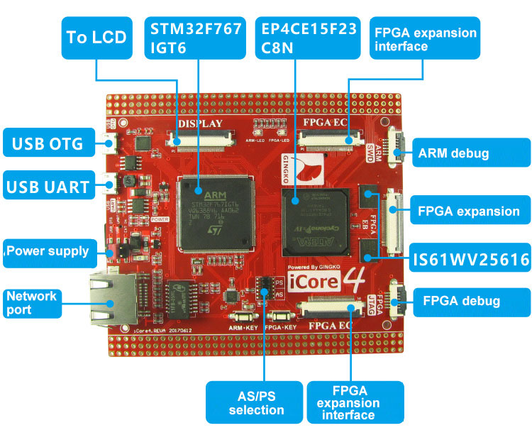
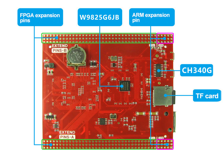
Product Characteristics: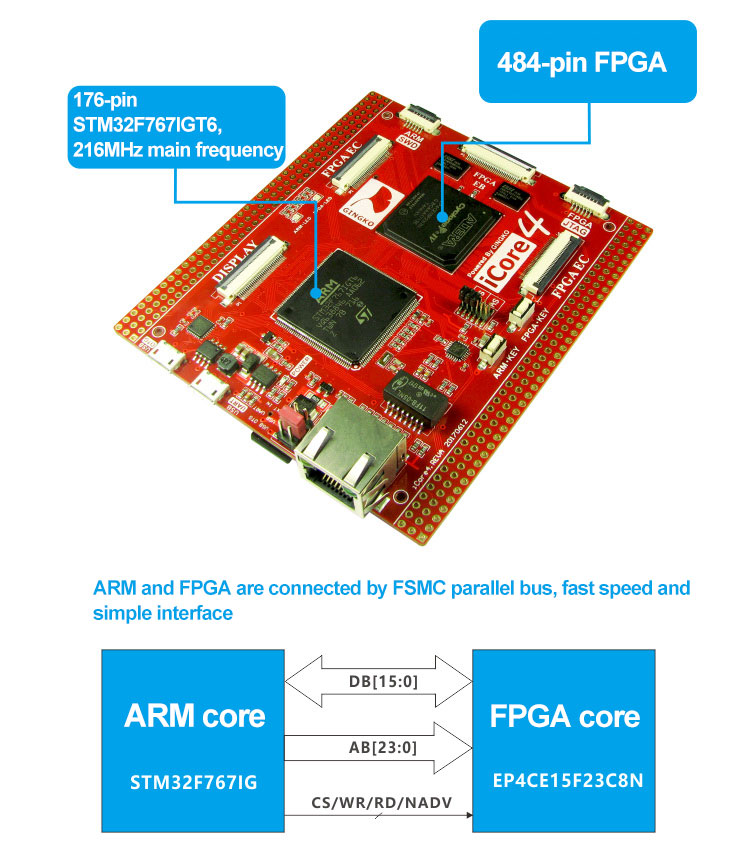
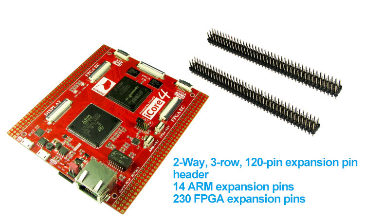
Package Included:
- 1 x Dual-Core Industrial Control Board For iCore4
- 1 x Set of Acrylic & Copper Pillars Screws
- 2 x Micro USB Data Cables
- 1 x Micro USB U Disk Reader Adapter
- 1 x Ethernet Cable
- 10 x Dupont Cables
- 1 x 128M TF Card (Inserted on the board)
- 2 x 3*40P 2.54 Spacing Pin Headers
- 1 x Precaution Paper
Note: Emulator is not included. 