| Quantity | 3+ units | 10+ units | 30+ units | 50+ units | More |
|---|---|---|---|---|---|
| Price /Unit | $38.47 | $37.69 | $36.51 | $34.94 | Contact US |
 Classic Version Industrial 5-Channel Data Recorder 16MB Memory Data Logger 4-inch Touch Screen with RS485 Interface
$252.79
 Classic Version Industrial 5-Channel Data Recorder 16MB Memory Data Logger 4-inch Touch Screen with RS485 Interface
$233.36
 Classic Version Industrial 4-Channel Data Recorder 16MB Memory Data Logger 4-inch Touch Screen with RS485 Interface
$213.93
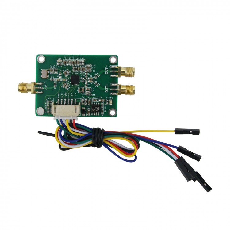
MAX2870 Module RF Signal Generator 23.5-6000MHz RF Signal Source 0.5PPM High Precision Low Noise PLL
Description:
MAX2870 is an ultra-wideband phase-locked loop (PLL), integrated voltage-controlled oscillator (VCO), and can work in integer and fractional-N modes. With an external reference clock oscillator and loop filter, the MAX2870 can form a high-performance frequency synthesizer, generating a clock in the frequency range of 23.5MHz to 6.0GHz (23.5-6000MHz), and can maintain excellent phase noise and spurious indicators. The internal multiple integrated VCO covering 3000MHz to 6000MHz and 1-128 output divider are used to realize clock output in an ultra-wide frequency range. The device provides dual-channel differential output drivers, which can be set to provide output power from -4dBm to +5dBm. Both outputs can be muted by software or hardware control.
MAX2870 is controlled by a 3-wire serial port and is compatible with 1.8V control logic. The device is packaged in a lead-free, RoHS-compliant 5mm x 5mm, 32-pin TQFN package, and operates in an extended temperature range of -40°C to 85°C.
Chip Characteristics:
1. Integer/fractional N frequency division mode
2. Manually or automatically select VCO
3. 23.5MHz to 6000MHz base frequency VCO
4. Output binary buffer/driver for expanding frequency range.
4.1. 1/2 /4 /8/16/32 /64/128.
4.2. 23.5MHz to 6000MHz.
5. High performance PFD.
5.1. In integer-N frequency division mode, 105MHz.
5.2. In fractional-N frequency division mode, 50MHz
6. Reference clock frequency up to 200MHz
7. +3.0V to +3.6V power supply
8. Two programmable amplitude outputs -4dBm to +5dBm
9. Analog and digital lock detection indication
10. Hardware and software shutdown control
11. Compatible with 1.8V control logic
Module Features:
1. Module power supply: 5V at 0.2A
2. Drive and power supply interface: 6P XH2.54 patch strip
3. Onboard default high-precision 25MHz 0.5ppm TCXO (can also be replaced by yourself or an external crystal oscillator)
4. Output frequency range: internal VCO fundamental frequency is 3-6GHz, below 3GHz is obtained by fundamental frequency division
5. Output interface: SMA-K (inner screw inner hole)
6.Provide STM32F1X driver test program
Package Included:
- 1 x Set of RF Signal Source