| Quantity | 3+ units | 10+ units | 30+ units | 50+ units | More |
|---|---|---|---|---|---|
| Price /Unit | $4.20 | $4.12 | $3.99 | $3.82 | Contact US |
 FMD Writer MCU Programmer Chip Programmer Tool Designed for 8-bit Microcontrollers Produced by FMD
$60.24
 Matrix:bit V2.0 Development Board Programming Control Board (Pink with Type-C Port) + Data Cable
$21.09
 Matrix:bit V2.0 Development Board Programming Control Board (Black with Type-C Port) + Data Cable
$21.09
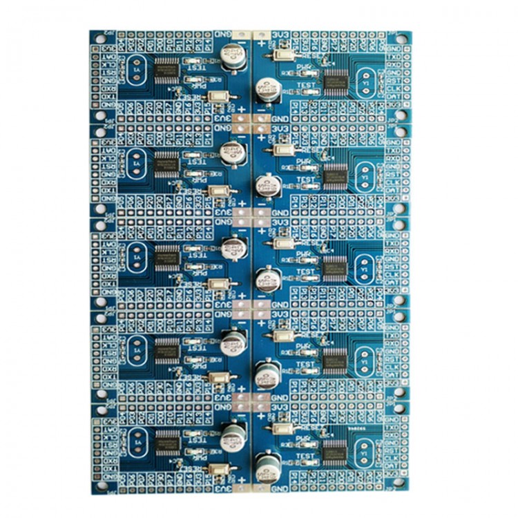
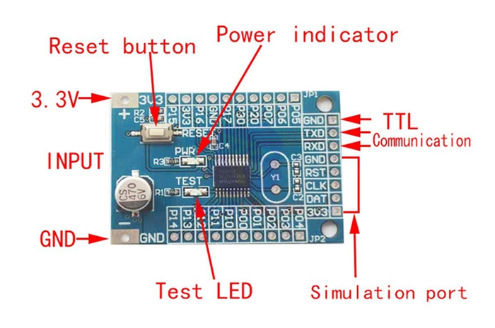
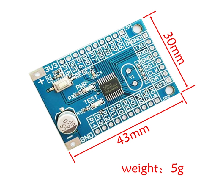
N76E003AT20 Development Board System Board Wireless Module DEMO Board
Features:
- Reserved 2.4G wireless module interface based on LT8920 chip (compatible with GWB and T400 wireless modules). It can be used as a demo board for 2.4G wireless module debugging and verification, and is accompanied by related development programs.
- IO port, power input, programming hole, and serial port are all exported for easy development.
- N76E003 replaces STM8S003, 51 core, development environment for Keil, It is very easy to get started.
- Users can download schematic diagram, 2.4G wireless module information, wireless module development test procedures, development environment software and other information. https://pan.baidu.com/s/1XX_b46w-2ixcMxAV3GZTiQ

Package Included:
- 1 x Development Board
N76E003 Introduction:
N76E003 is a high-speed 1T 8051 MCU series product, providing 18 KB Flash ROM, configurable Data Flash and high-capacity 1 KB SRAM. It supports 2.4V to 5.5V wide working voltage and -40℃ to 105℃ working temperature, and have high anti-interference ability 7KV ESD / 4KV EFT.
N76E003 provides up to 18 I / O pins in a 20 pin package. Peripherals include dual serial ports, SPI, I2C, and 6-channel PWM outputs. Built-in high accuracy 16 MHz RC crystal with <2% error superior to similar products and high resolution 8-channel 12-bit ADC. And with self-wake-up, under-voltage detection and other functions. Available in small TSSOP20 (4mm * 6.5mm) and QFN20 (3mm * 3mm) packages with high performance and design flexibility.
Characteristics:
CPU:
- Full static 8-bit 1T 8051 core CMOS MCU.
- Instruction set is fully compatible with MCS-51.
- 4-level priority interrupt configuration.
- Double data pointers (DPTRs)
Working Conditions:
- Wide voltage operating range from 2.4V to 5.5V.
- Wide operating frequency up to 16MHz.
- Industrial-grade operating temperature -40℃ to + 105℃.
Memory:
- Up to 18K bytes of APROM user program code area.
- Configurable 4K / 3K / 2K / 1K / 0K byte LDROM boot code area, users can flexibly configure usage
- All FLASH areas are separated into 128-byte pages.
- Built-in IAP programming function.
- Code encryption function.
- 256 bytes of on-chip direct access to RAM.
- Extra 768 bytes of on-chip indirect access RAM (XRAM) are read and written by MOVX instructions
Clock Source:
- 16 MHz high-speed internal oscillator with ±1% accuracy level at 5.0V power supply. Full working condition range ±2% accuracy level.
- 10 kHz low-speed internal oscillator.
- Support for external clock input.
- Support on-the-fly function of system clock.
- Supports software-configurable clock division up to 1/512.
Functions:
- Up to 17 standard general-purpose pins, and an additional input-only pin. All output pins can be configured by software with two output slew rates
- Two sets of 16-bit timer / counters 0 and 1, compatible with standard 8051
- A group of 16-bit timers 2 with 3 input capture functions, 9 input pins are available for selection
- A set of 16-bit auto-reload timer 3, which can be used to configure the baud rate of the serial port UART
- A set of 16-bit PWM count interrupts
- One watchdog (WDT), with internal 10kHz independent clock as clock source
- A set of self-wake-up timers (WKT) for autonomous wake-up in low-power modes
- Two full-duplex serial ports with frame error detection and automatic address recognition. The TXD and RXD pins of UART0 can be changed by software.
- A group of SPI bus, when the system clock is 16MHz, the highest transfer rate of the master mode and slave mode can reach 8Mbps
- A set of I2C bus, the maximum transfer rate of master mode and slave mode can reach 400kbps
- Three pairs, 6-channel pulse width modulator (PWM), 10 output pins can be selected, 16-bit resolution, with different operating modes and fault brake function
- Up to 8-channel pin interrupt function can be configured, all I / O ports support this function, and edge or level trigger can be configured by software
- A set of 12-bit ADCs with a maximum conversion rate of 500ksps, it is easier to control the motor function by hardware startup and comparison of the conversion results
Power Management Module:
- Two power-saving modes: idle mode and power-down mode
Power Monitoring:
- Under-voltage detection (BOD) is used to detect the low voltage of system power supply, 4 levels of voltage selection, configurable interrupt or reset response
- Power-on reset (POR)
- Strong ESD and EFT capabilities
Development Tools:
- On-chip debugging (OCD simulation) based on KEILTM development environment
- In-Circuit Programming (ICP Programming)
- In-System Programming (ISP programming), programming chip through UART
Compared with STM8S003F3P6:
STM8S003F3P6: a total of 20 pins, supporting up to 16 GPIOs and 16 external interrupts. 2pcs 16-bit timers [TIM1 / TIM2] can output up to 3 PWM signals. 5 ADC channels support SPI / I2C / UART. 8KBYTE FLASH, 1K RAM, 128 BYTE EEPROM. With built-in 16M high-speed oscillator, WDG and so on.
From the perspective of the performance of device alone, N76E003AT20 has more classic advantages:
• 1T / 8051: 1T value MCU, 8051 is the classic core we are more familiar with;
• 18KB Flash ROM: better than 8KB Flash, and all 18KB of flash space can be used as data storage space;
• 1024B SRAM;
• 17 + 1 inputs: better than supporting up to 16 GPIOs;
• 2 * UART, I2C, SPI: better than SPI / I2C / UART (one more UART);
• 8ch of 12bit ADC: better than 5-channel 10bit ADC;
• 6ch of individual duty PWM: better than 3 PWM outputs;
• 10KHz LIRC for WDT reset / WKT;
• 16MHz HIRC ± 1% Room temp. ± 2% full condition;
• -40 ~ 105 ℃ wider temperature range;
• Wider supply voltage range from 2.4V to 5.5V;
• TSSOP20 / QFN20;
• ESD & EFT: HBM / 8KV MM / 400V, Over 4KV, excellent ESD and EFT, anti-interference and ESD protection capabilities.