| Quantity | 3+ units | 10+ units | 30+ units | 50+ units | More |
|---|---|---|---|---|---|
| Price /Unit | $327.25 | $320.57 | $310.55 | $297.20 | Contact US |
 BU-5 Bluetooth Module Radio Bluetooth Adapter Unit for Yaesu FTM-150R FTM-510DR Transceiver
$55.79
 STF10M1000M-25 RF Power Amplifier 10-1000MHz 25W-30W Wideband RF Amplifier without Radiator and Cooling Fan
$490.69
 STF10M1000M-25 RF Power Amplifier 10-1000MHz 25W-30W Wideband RF Amplifier with Radiator and Cooling Fan
$543.48
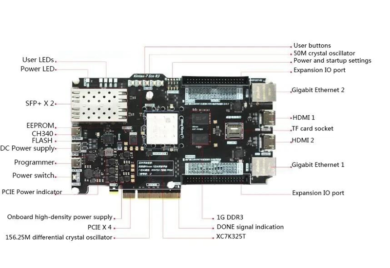
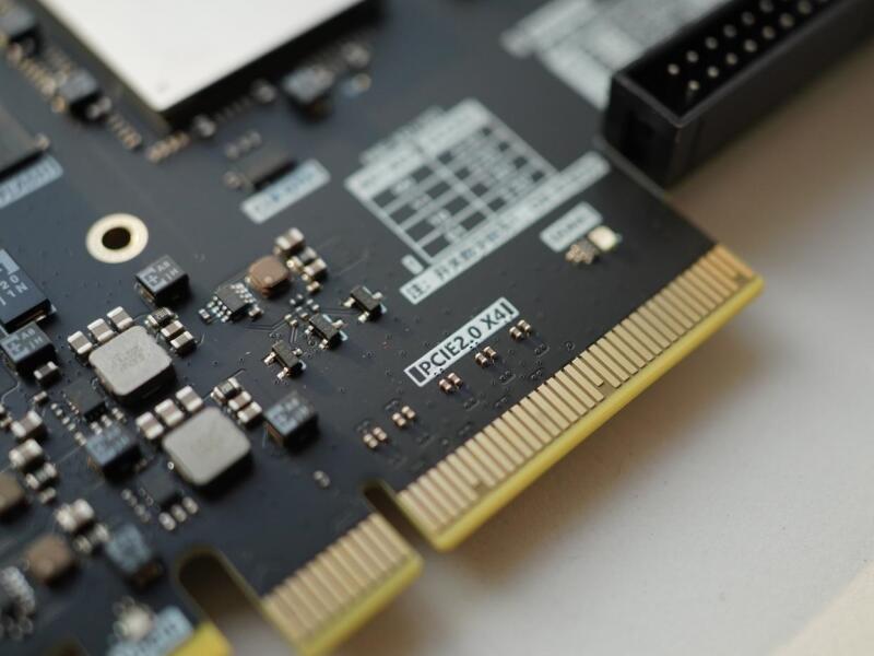
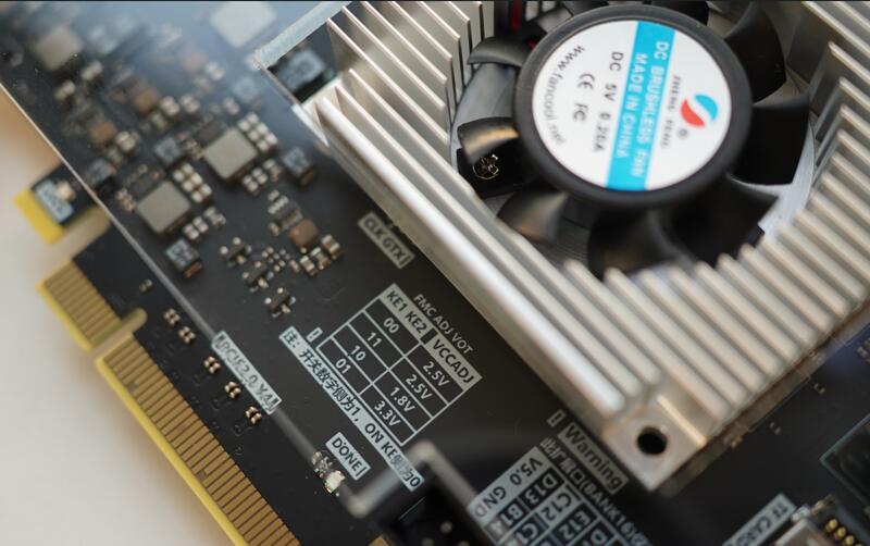
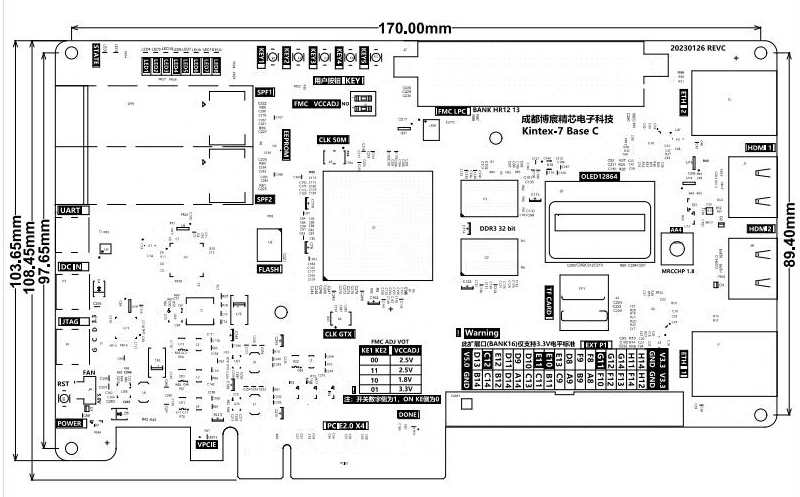
XC7K325T Kintex 7 Base Development Board with 10G Optical Module FPGA Development Board Onboard 0.96-inch OLED for Xilinx
Chip Parameters:
- Main chip: XC7K325T-2FFG6761
- Chip level: industrial
- Clock recommended maximum speed: PLL/MMCM recommended maximum 709M
- DDR specification model: 2pcs MT41K256M16TW-107, 1GB (bytes), recommended maximum 1600M
- Logic unit (LC): 326080
- Slices: 50950
- DSP unit multiplier: 840
- Trigger: 407600
- RAM: 160,20Kbit
- Component temperature range: -40 ~ 85℃
- Speed class: -2
- Number of GTX: 8
Development Board Parameters:
- Power supply mode: Type-C 9-12V/2A power supply
- Heat dissipation interface: onboard one GH1.25-3P connector radiator interface
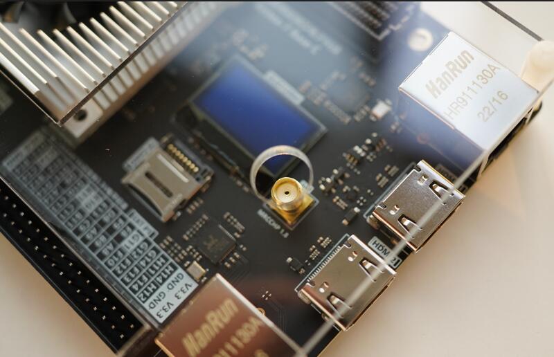
- Clock resources: 50M single-end crystal oscillator, 156.25M differential crystal oscillator and one channel SMA clock interface
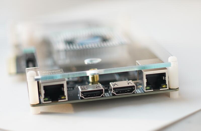
- Ethernet: two gigabit RGNII, model of RTL8211E-VL, and another RTL8211E-VB
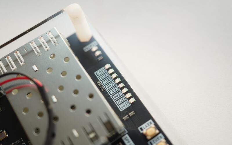
- User button: five user buttons, one power-on/reset, support global reset and reconfiguration of chips
- Debugger: Type-C interface downloader for Xilinx, support online debugging and download
- Serial port: one channel Type-C interface CH340 serial port
- SD card: one clamshell TF card slot, support SPI interface
- HDMI-interface: two channel support output up to 1080 at 60Hz
- Onboard LED: two power status LED, eight FPGA LED, DONE, PCIE power supply
- Setting switch: one voltage dial switch for setting the LA differential pin of the FMC interface
- Onboard FLASH: MX25L25645G particle, 32MByte space
- EEPROM: one 24C02 EEPROM memory chip
- PCIE interface: PCIE2.0 x 4 (4lane GTX. 4RX TX)
- Onboard OLED module: 0.96-inch SSD1306 driving OLED module, 128x64 mono
- Expansion IO port: standard FMC LPC interface and 40P standard 2.54 dual row expansion port; FMC includes LA (34 pairs of differential + 2 pairs of clock differential) and 1 pair of GTX; The 40PIN 2.54 expansion IOs only includes 34 3.3V single ended IOs.
- Optical communication interface: 2 channels SFP+, support 10G optical communication (only for optical communication version)
- Note:
FMC can configure BANK12, 13 voltage to be 1.8/2.5/3.3V using dial switches.
FMC uses ANK12 and 13, as HR BANK, LVDS only supports 2.5V LVDS_25.
The 40P 2.54 expansion port uses BANK16 as the HR BANK, with a fixed voltage of 3.3V single ended.
Package Included:
- 1 x Development Board
- 2 x Type-C Data Cable
- 1 x 9V/2A Type-C Power Adapter
- 1 x 10G Optical Module
- 1 x LC Jumper Line

